홈
Communication
Newsroom
Semiconductor
SKC Makes its Debut at MWC, Showcasing Vision for Key AI Data Center Solutions
lExhibiting real semiconductor glass substrates at MWC 2025, highlighting key AI data center solutionslReducing power consumption and thickness by more than 50% compared to conventional substrates while enhancing data processing speed by 40%lPioneering world’s first commercialization of glass substrates by year-end, driving advancements in AI technologySKC (CEO Woncheol Park) will showcase its glass substrates at Mobile World Congress 2025 (MWC2025), the world’s largest mobile exhibition, taking place from March 3 to 6 (local time).SKC will exhibit its glass substrates in the AI DC (AI Data Center) zone within the exhibition hall operated by SK Telecom. Under the theme “Innovative AI Accelerates the Future,” the exhibition will feature key technologies related to AI data centers (AI DC) and the latest research advancements in AI-powered communication infrastructure.Glass substrates will be showcased as a key technology essential for processing large-scale data in the AI DC zone. Notably, they will be exhibited alongside SK hynix’s high-bandwidth memory (HBM3E) and high-performance SSD storage for data centers, presenting a comprehensive AI solution.Glass substrates enable the implementation of ultra-fine circuits and can incorporate various components, such as MLCCs, allowing large-capacity central processing units (CPUs) and graphics processing units (GPUs) to be mounted on their surface. When applied to semiconductor packaging, glass substrates reduce power consumption and package thickness by more than half while increasing data processing speed by 40% compared to conventional substrates.An SKC representative stated, “As the world’s first company to commercialize semiconductor substrates, we are proud to showcase our technological excellence on the global stage at MWC 2025, following our successful appearance at CES 2025”. They added, “We look forward to contributing to the advancement of AI technology, which is capturing global attention, through the successful commercialization of glass substrates by the end of the year.” [End]
2025-03-04
SKC Showcases Glass Substrates for AI Data Center at CES 2025
l
Exhibiting actual semiconductor glass substrates at CES 2025, showcasing
their potential as a key material for AI data centers.l
Highlighting advanced glass substrate technology for AI semiconductors
and participating in presentation sessions.l Reaffirming its technological leadership as
the world’s first to commercialize glass substrates.
SKC (CEO Woncheol Park) will unveil its glass
substrates, widely regarded as a “game changer” in the semiconductor industry,
at CES 2025—the world’s largest consumer electronics and IT exhibition—scheduled
to take place from January 7 to 10 (local time) in Las Vegas, USA.
SKC exhibits actual glass substrates in the AI Data Center (AI DC) zone
of the exhibition hall jointly operated by four SK Group affiliates (SKC, SK
hynix, SK telecom, and SK enmove). Operated under the theme of “Innovative AI, Sustainable Tomorrow,” the SK
exhibition hall is divided into three zones: AI DC, AI Services, and AI
Ecosystems.
During the exhibition, glass substrates will be presented as a solution
to enhance the speed of AI servers handling large-scale data. A visualization
of their application in AI data centers will provide visitors with a tangible
understanding of how the substrates are utilized in practice.
In addition to the exhibition, a presentation will highlight the
advantages of glass substrates. Absolics, an SKC-invested affiliate in the glass
substrate business, will participate in a session titled “Cutting-edge Hardware
and Software for AI Semiconductors,” offering insights into the future
development of AI solutions driven by glass substrate technology.
Glass substrates offer several advantages, including the ability to
implement ultra-fine circuits and house various components, such as MLCCs, enabling
large-capacity CPUs and GPUs to be mounted on their surface. This leads to a
40% increase in data processing speed compared to conventional substrates,
while reducing power consumption and package thickness by over 50%. Applying glass substrates to AI data centers can significantly
reduce their physical footprint and energy consumption.
SKC has completed the world’s first mass-production facility in Georgia,
USA, and is accelerating its commercialization efforts. Last year, SKC secured USD
75 million in production subsidies and USD 100 million in R&D grants from the
U.S. government, recognizing its technological innovation.
An
SKC representative stated, “As the first company in the world to commercialize
semiconductor substrates, CES provides an opportunity to once again showcase our
technological excellence on a global stage.” They added, “We will further
solidify our technological edge through glass substrates amid the increasingly
fierce competition in the semiconductor industry.” [End]
2025-01-10
SKC assigns fine ceramics business to Hahn & Company
● Signing a business assignment deal with PEF manager Hahn & Company··· at 360BN won●SKC cranking up a business overhaul, focused on semiconductors, proprietary high-value materials and componentsSKC (CEO: CEO: Woncheol Park) assigned the fine ceramics business of its chip material-producing subsidiary SK Enpulse to Hahn & Company, a top-tier private equity fund (PEF) managers in Korea.SK Enpulse announced on the 31st that the company convened a board meeting on the 30th where they resolved to assign its fine ceramics business to Hahn & Company for 360 billion won. After the board meeting, the two companies signed a business assignment agreement to that effect. SK Enpulse is expected to undergo necessary procedural steps including an extraordinary shareholders’ meeting next month and close the deal next January.Fine ceramics refer to materials based on highly pure inorganic compounds and processed to feature better electrical properties and durability than conventional ceramic materials. SK Enpulse supplies in the market parts based on well-known fine ceramics including alumina (Al2O3), silicon (Si), silicon carbide (SiC), and quartz which are required for a variety of semiconductor and display manufacturing processes. In so doing, SK Enpulse has contributed to raising the ratio of homegrown chip materials and components in the market.Hahn & Company that will acquire the fine ceramics business from SK Enpulse is the biggest PEF investment manager in Korea. Since its incorporation in 2010, Hahn & Company has acquired over 30 promising Korean companies and prospected for new growth engines, adopting the first-ever bolt-on strategy in Korea to improve their business fundamentals and ramp up market capitalization. Hahn & Company is expected to shore up global competitiveness of the fine ceramics business by ensuring employees’ job security and making additional investments after the assignment.SKC is accelerating the overhaul of its semiconductor business with focus on new high-value items, selling the basic chipmaking material business of SK Enpulse including wet chemical and washing operations, purchasing equity in the U.S. chip packaging solution provider Chipletz, and acquiring semiconductor test solution company ISC. Furthermore, SKC vows to further enhance its business competitiveness by seeking to commercialize the world’s first semiconductor glass substrate for high-performance computing applications and identify additional M&A opportunities.“SKC will use the sale proceeds of the fine ceramics business as funding resource to push the competitive edge of the chip material and component business to a new height,” said an official at SKC. “We will build solutions on our proprietary technologies and become a game changer in the global chip material and component market.” [End]
2023-10-31
SKC closes acquisition of global chip test solution provider ISC
● Winding up the acquisition procedure on Oct. 4··· Incumbent ISC CEO Kim Jeong-ryeol and CEO Kim Jong-woo of SK Enpulse to jointly take the helm●ISC to emerge as a pivotal block of the chip business··· vowing to post 3 trillion won in chip materials sales by 2027, reshuffling its product portfolio with high-value itemsISC, a global leader of chip test solutions, is making a fresh start as a subsidiary of SKC (CEO: Woncheol Park).SKC fully paid the stock purchase price on October 4, wrapping up the acquisition of ISC. Together with incumbent CEO Kim Jeong-ryeol, CEO Kim Jong-woo of SK Enpulse will be appointed as a joint CEO. Signing a stock purchase agreement (SPA) with ISC’s biggest shareholder, Helios Private Equity Fund No.1 this July, SKC has worked on steps to close the deal, including submission of corporate consolidation report in Korea and elsewhere. SKC also participated in ISC’s recapitalization to raise its equity ratio to 45%, laying down groundwork for further growth.Incorporated in 2001, ISC has built its portfolio around test sockets for testing the electrical properties of semiconductor chipsets. Test sockets are regarded as a key consumable in the downstream segment of chipmaking process. In particular, as leading chipmakers try to advance packaging technologies to improve the performance of chipsets, demand for test chips is rising rapidly, implying significant potential growth way forward.ISC succeeded in commercializing the world’s first silicone-based test sock in 2003, currently dominating the market with over 50% market share. ISC also excels in technological prowess, holding the industry record of more than 500 patents. Let alone silicone sockets, ISC possesses a variety of test solutions, including copper alloy-based pogo sockets that are conventional electrical property test sockets and interface boards.SKC aims to facilitate the growth of ISC as a key building block of its chip material business. In addition to becoming an investment destination by scaling up its existing business, ISC is expected to create synergy by forging technological collaboration with semiconductor substrate business and commercializing integrated solutions. Furthermore, SKC vows to work on additional M&A deals in the semiconductor sector to boost the semiconductor sales to 3 trillion won by 2027.Prior to the ISC deal, SKC sold off its basic semiconductor material business involving wet chemical and washing to local companies in China the previous month. SKC also invested in Chipletz in the United States in a bid to enhance its business foundation for cutting-edge chip packaging solutions and dedicated a semiconductor substrate production plant in the State of Georgia, putting in high gears its chip business migration to high-value materials/components.“Acquiring ISC, SKC is embarking on a full-scale migration of semiconductor business portfolio to high-value products and solutions,” said an official at SKC. “To stimulate the growth of ISC, we will render active support, identifying new business opportunities and launching drastic investment initiatives.”
2023-10-04
SK enpulse Sells Its Semiconductor Basic Materials Business
● Wet chemical & cleaning business is sold to local companies: Yaker Technology and Sunyang Shinjin.●SKC’s semiconductors materials/parts will continue the accelerated innovation centered on its high-value-added businesses.SK enpulse, an invested subsidiary of SKC (CEO & President Woncheol Park) in the semiconductor materials business, is selling its semiconductor front-end process basic materials business.On September 12, SK enpulse held a board meeting that decided to sell two of its businesses in China to local companies. The wet chemical business will be sold to the local semiconductor/display materials company Yaker Technology, and the cleaning business will be sold to the investment company Sunyang Shinjin. The sale amounts to approximately KRW 88 billion, including SK enpulse’s 75% stake in the wet chemical business and 90% in the cleaning business. SK enpulse signed share purchase agreements (SPA) with Yaker Technology and Sunyang Shinjin immediately after the board meeting.Yaker Technology, acquiring the wet chemical business, is a large company listed on the Shenzhen Stock Exchange in China, with its operations involving special gases for semiconductors/displays and photoresistor business. Sunyang Shinjin has invested in and owns equipment/parts manufacturers for semiconductor processes.SKC integrated its semiconductor materials/parts businesses into SK enpulse early this year, seeking to continuously expand high-value-added materials business areas for semiconductor front-end processes, including CMP pads and blank masks. Additionally, the company is entering the semiconductor back-end process scene. Last month, SKC signed an agreement to acquire ISC, a global leader in semiconductor test solutions, and plans to complete the world’s first glass substrate mass production facility for high-performance semiconductor packaging in Georgia, USA, through Absolics Inc. at the end of this year.The sale is part of a business restructuring focused on high-value-added materials/parts. An SK enpulse executive said, “Our decision to sell existing businesses was made ambitiously to centralize our efforts on the high-value-added materials and parts business that are essential in the future semiconductor industry,” and added, “We will continue to strive for business model innovation.” [End of document]
2023-09-13
SKC invests in Chipletz, a rising star of the U.S. chip packaging industry
● Securing about 12% equity in Chipletz, a tech. firm spun off from AMD by joining its Series B funding as a strategic investor● Eyeing synergy with high-performance computing chip glass substrate business ··· accelerating the global expansion of back-end chip process businessSKC (President & CEO Woncheol Park) invests in Chipletz, a U.S. chip packaging startup. Chip packaging refers to the back-end process in which chips supporting different functions respectively such as CPU, DRAM, etc. are seamlessly connected with each other, and it is emerging as a key determinant of chipset performance. The Chipletz investment will allow SKC to further accelerate the global expansion of its chip back-end process business.SKC announced on the 10th that the Company would acquire about 12% stake in Chipletz in its Series B funding round. Exact equity ratio will be finalized when Chipletz’s Series B funding is closed. The two companies agreed not to disclose the amount of investment. After incorporating Absolics, a chip glass substrate manufacturer, in 2021 which is scheduled to dedicate its Phase 1 production facility by the end of this year, SKC rolls out full-scale partnership with a global tech. firm to access innovative chip packaging technology.Chipletz was launched as a CIC (company in company) of AMD, U.S.-based global chip maker, in 2016 and spun off from the parent company 5 years after in 2021. Chipletz has a full package of architectural engineering and technology development know-how for cutting-edge semiconductor substrates as well as access to a network of big-name customers. AMD and Taiwan’s ASE, the world’s largest OSAT (outsourced semiconductor assembly and test) provider, already top the shareholders list of Chipletz, with stakes in the company.Co-founder and CEO Bryan Black of Chipletz is a chip packaging expert who worked for Intel and AMS for more than 20 years. In particular, he is named as one of the most foremost authorities on next-gen. chip packaging technologies which are essential for AI computing such as ‘3D packaging’ that connects multiple heterogeneous chips in a 3D architecture. Other management leaders of Chipletz including CTO Michael Su, also one of the co-founders, and Vice President of Product Engineering Michael Alfano are also known for their long-standing careers in the chip packaging sector.Incorporating Absolics in 2021, SKC is endeavoring to roll out the world’s first commercial glass substrate for high-performance computing chips. Chips packaged with glass substrate are known to be the game changer of the market, as they can drastically improve data processing throughput of chipsets while cutting power consumption by half. SKC’s Phase 1 production facility under construction in Geogia, U.S.A. is coasting along without any setback toward the goal of completion by year-end.The investment will enable SKC to forge strong partnership with Chipletz in the field of chip packaging. SKC vows to combine its glass substrate production capacity with Chipletz’s engineering know-how, architectural and other relevant technologies, and access to a network of customers, etc. to build a differentiated ‘chip packaging solution ecosystem.’ Furthermore, the two companies will join forces in fostering R&D and responding to the U.S. CHIPS & Science (Creating Helpful Incentives to Produce Semiconductors and Science) Act of 2022.As the fabrication approach to increasing capacity by narrowing linewidth has met its limit in the semiconductor industry, the packaging technology that combines multiple chips seamlessly to render higher performance is getting increasingly important. SKC, which is already expanding a suite of high-value components for front-end process such as CMP pad, blank mask, etc. via its investee SK enpulse, will significantly enhance its packaging business infrastructure for the future by investing in Chipletz next to the commercialization of chip glass substrates and the acquisition of ISC, a packaging test solutions provider.“The strategic investment in Chipletz that has a global top-tier packaging architecture technology enhances our competitive edge for chip materials and components by a notch,” an official at SKC said. “A combination of SKC’ proprietary technologies and manufacturing capacity with Chipletz’s packaging engineering capability will be a game changer in the chip back-end process market.” [End]Chipletz website: www.chipletz.com
2023-09-11
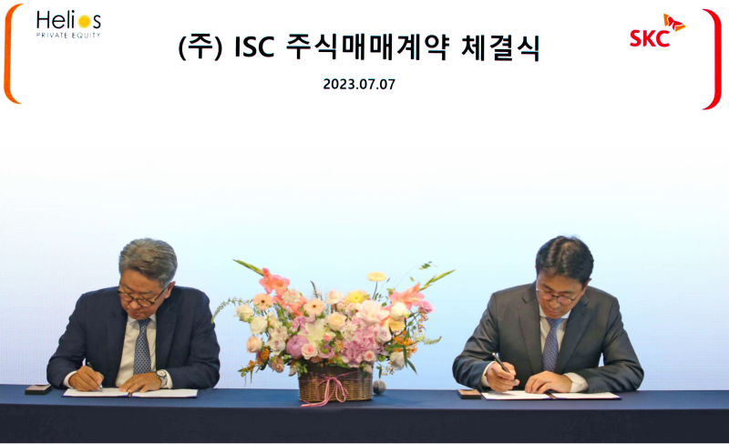 SKC decided to acquire ISC, a semiconductor test solution provider
● A KRW 522.5 billion investment was decided in the board of directors meeting on July 7, including the acquisition of the largest shareholder’s stake (KRW 347.5 billion) and new shares (KRW 175 billion).● After the acquisition of ISC, the world’s number one manufacturer of silicone rubber sockets for testing semiconductor chipsets, SKC will further search for additional growth engines.● Following the glass substrate business, SKC has added a high value-added business for the semiconductor back-end process, seeking global expansion to Vietnam (ISC production base).SKC (CEO & President Woncheol Park) has acquired ISC, a global semiconductor test solution provider, to add a new growth engine to its semiconductor materials/parts business, one of its three growth pillars, along with EV battery and eco-friendly materials.On July 7, SKC held a board of directors meeting and decided to acquire 35.8% of ISC’s shares owned by the current largest shareholder Helios Private Equity Fund I for KRW 347.5 billion and also to acquire ISC’s newly issued shares worth KRW 200 billion jointly with Helios Private Equity. SKC is investing KRW 175 billion in ISC’s new shares, expanding its total stake to 45%. Immediately after the board of directors meeting, the Stock Purchase Agreement (SPA) and the Share Subscription Agreement (SSA) were signed.SKC plans to finance funds for the acquisition without compromising its existing investment capacity or being funded from outside. ISC will start anew as an SKC subsidiary upon completing the necessary procedures, such as filing the corporate merger and obtaining relevant approvals.The acquisition of ISC will significantly strengthen SKC’s semiconductor post-process materials/parts business. ISC was founded in 2001 and is known for test sockets, its main product, used to test electrical characteristics of packaged semiconductor chipsets, which are essential consumables in the semiconductor back-end process. Also, it should be noted that its future growth potential is deemed excellent because demand for test sockets is growing rapidly as the packaging technology of major semiconductor manufacturers is advancing to improve the performance of their chipsets.In 2003, ISC became the first in the world to commercialize test sockets utilizing silicone rubber materials and continues to hold an overwhelming first place in this market today with over half of the market share. It also has strong technological capabilities with more than 500 patents, the most in the industry. According to the semiconductor industry, silicone rubber sockets already account for over 80% of memory semiconductor test sockets and are expected to further expand rapidly in the non-memory market as well.In addition to silicone rubber sockets, ISC has a wide range of test solutions, such as pogo sockets made of copper alloy previously used for electrical characteristic testing sockets, burn-in test sockets, and interface boards. SKC plans to utilize ISC as a platform to expand its semiconductor materials/parts business. To this end, it plans to actively pursue additional mergers and acquisitions (M&A) as well as grow the existing business after the acquisition.Through this acquisition, SKC will further strengthen its portfolio in the semiconductor back-end process and carry on with its business model innovation efforts. SKC already has CMP pads and blank masks for the front-end process through its subsidiary, SK npulse. Also, through Absolics Inc., SKC is working to commercialize semiconductor glass substrates, which are considered a game changer in the packaging market of the back-end process.In addition, SKC is expected to position itself as a materials/parts solution enterprise offering a comprehensive high-value-added product lineup in both the front-end and back-end processes. Its global expansion will further be accelerated to Vietnam, the production base of ISC, following the SK nexilis copper foil manufacturing facility in Malaysia.An SKC executive said, “This acquisition has served to further strengthen our semiconductor back-end process materials/parts business strengthening our semiconductor back-end process materials/parts business, allowing us to achieve another business model innovation as a global ESG materials solution enterprise and secure additional footholds for growth” and added, “We will contribute to the continuous growth and happiness of both SKC and ISC and to enhance the competitiveness of the semiconductor industry in South Korea as well.ISC Stock Purchase Agreement Signing Ceremony (July 07, 2023)[SKC announced on July 7 its acquisition of ISC, a semiconductor test solution provider. SKC CEO & President Woncheol Park (right) and CEO & President Che Moe Chun of Helios PE, the largest shareholder of ISC, are signing the agreement at the SPA signing ceremony.]
2023-07-07
SKC decided to acquire ISC, a semiconductor test solution provider
● A KRW 522.5 billion investment was decided in the board of directors meeting on July 7, including the acquisition of the largest shareholder’s stake (KRW 347.5 billion) and new shares (KRW 175 billion).● After the acquisition of ISC, the world’s number one manufacturer of silicone rubber sockets for testing semiconductor chipsets, SKC will further search for additional growth engines.● Following the glass substrate business, SKC has added a high value-added business for the semiconductor back-end process, seeking global expansion to Vietnam (ISC production base).SKC (CEO & President Woncheol Park) has acquired ISC, a global semiconductor test solution provider, to add a new growth engine to its semiconductor materials/parts business, one of its three growth pillars, along with EV battery and eco-friendly materials.On July 7, SKC held a board of directors meeting and decided to acquire 35.8% of ISC’s shares owned by the current largest shareholder Helios Private Equity Fund I for KRW 347.5 billion and also to acquire ISC’s newly issued shares worth KRW 200 billion jointly with Helios Private Equity. SKC is investing KRW 175 billion in ISC’s new shares, expanding its total stake to 45%. Immediately after the board of directors meeting, the Stock Purchase Agreement (SPA) and the Share Subscription Agreement (SSA) were signed.SKC plans to finance funds for the acquisition without compromising its existing investment capacity or being funded from outside. ISC will start anew as an SKC subsidiary upon completing the necessary procedures, such as filing the corporate merger and obtaining relevant approvals.The acquisition of ISC will significantly strengthen SKC’s semiconductor post-process materials/parts business. ISC was founded in 2001 and is known for test sockets, its main product, used to test electrical characteristics of packaged semiconductor chipsets, which are essential consumables in the semiconductor back-end process. Also, it should be noted that its future growth potential is deemed excellent because demand for test sockets is growing rapidly as the packaging technology of major semiconductor manufacturers is advancing to improve the performance of their chipsets.In 2003, ISC became the first in the world to commercialize test sockets utilizing silicone rubber materials and continues to hold an overwhelming first place in this market today with over half of the market share. It also has strong technological capabilities with more than 500 patents, the most in the industry. According to the semiconductor industry, silicone rubber sockets already account for over 80% of memory semiconductor test sockets and are expected to further expand rapidly in the non-memory market as well.In addition to silicone rubber sockets, ISC has a wide range of test solutions, such as pogo sockets made of copper alloy previously used for electrical characteristic testing sockets, burn-in test sockets, and interface boards. SKC plans to utilize ISC as a platform to expand its semiconductor materials/parts business. To this end, it plans to actively pursue additional mergers and acquisitions (M&A) as well as grow the existing business after the acquisition.Through this acquisition, SKC will further strengthen its portfolio in the semiconductor back-end process and carry on with its business model innovation efforts. SKC already has CMP pads and blank masks for the front-end process through its subsidiary, SK npulse. Also, through Absolics Inc., SKC is working to commercialize semiconductor glass substrates, which are considered a game changer in the packaging market of the back-end process.In addition, SKC is expected to position itself as a materials/parts solution enterprise offering a comprehensive high-value-added product lineup in both the front-end and back-end processes. Its global expansion will further be accelerated to Vietnam, the production base of ISC, following the SK nexilis copper foil manufacturing facility in Malaysia.An SKC executive said, “This acquisition has served to further strengthen our semiconductor back-end process materials/parts business strengthening our semiconductor back-end process materials/parts business, allowing us to achieve another business model innovation as a global ESG materials solution enterprise and secure additional footholds for growth” and added, “We will contribute to the continuous growth and happiness of both SKC and ISC and to enhance the competitiveness of the semiconductor industry in South Korea as well.ISC Stock Purchase Agreement Signing Ceremony (July 07, 2023)[SKC announced on July 7 its acquisition of ISC, a semiconductor test solution provider. SKC CEO & President Woncheol Park (right) and CEO & President Che Moe Chun of Helios PE, the largest shareholder of ISC, are signing the agreement at the SPA signing ceremony.]
2023-07-07
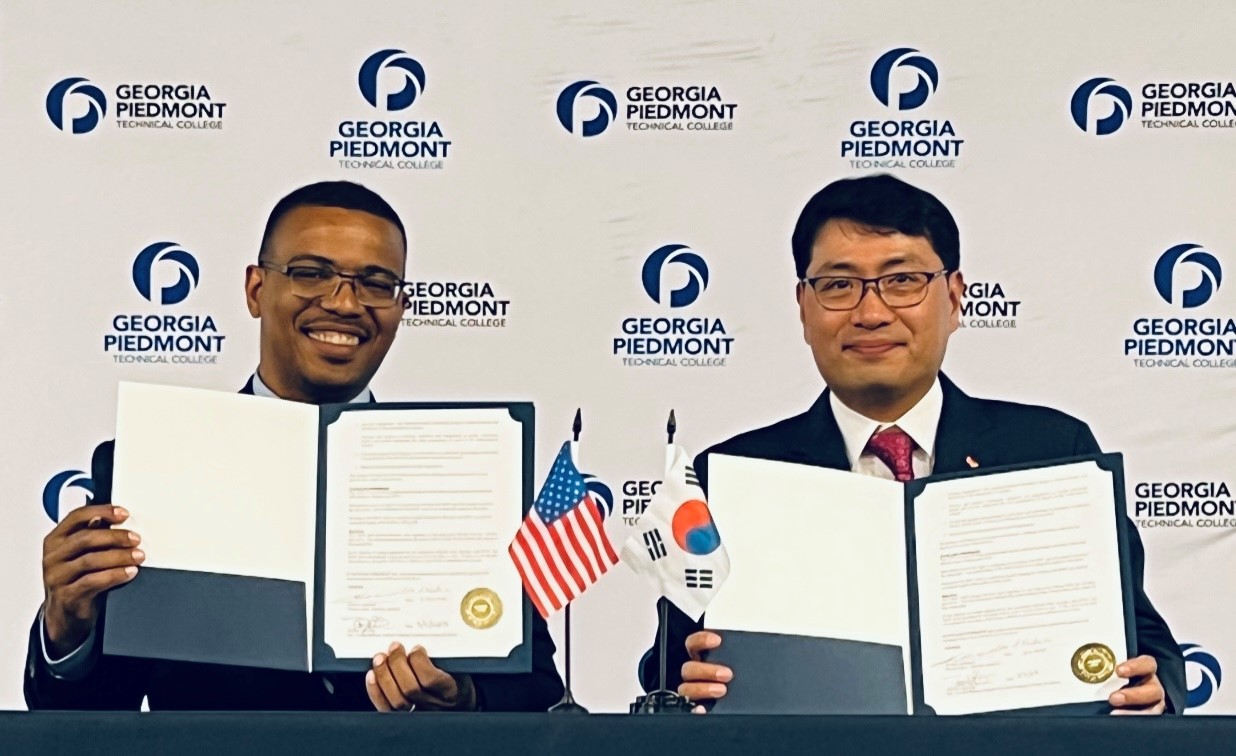 Absolics Inc. partners with a local U.S. educational institution to develop human resources for semiconductors.
● Absolics Inc. signed an industry-academia collaboration agreement with Georgia Piedmont Technical College to set up an education/training program and jointly structure the curriculum.● The collaboration is aimed to develop technical talent that the glass substrate business could benefit from and contribute to reinforce the competitiveness of the local semiconductor industry ecosystem.Absolics Inc., a semiconductor glass substrate business in which SKC (CEO & President Woncheol Park) has invested, partnered with a local U.S. educational institution to develop human resources for the semiconductor industry.Absolics Inc. signed an industry-academia collaboration MOU with Georgia Piedmont Technical College (GPTC) on March 9 (local time) to jointly set up an education/training program for human resources development of the semiconductor industry. The signing ceremony, held at GPTC’s Newton Campus in Covington, Newton County, Georgia, was attended by key officials from both sides including Absolics Inc. CTO Seongjin Kim and GPTC President Tavarez Holston.This MOU will serve as a basis for Absolics Inc. and GPTC to structure an education/training curriculum of industry-academia collaboration customized for jobs such as semiconductor quality management and defect analysis. The goal sought through this arrangement is to develop the human resources that the semiconductor glass substrate business need and contribute to reinforcing the competitiveness of the overall local semiconductor industry ecosystem in the long term.Absolics Inc. is the first company in the world to promote the semiconductor glass substrate business that is building a manufacturing facility on an SKC inc. site in Georgia since last November. A first-phase investment of USD 240 million was made to complete the manufacturing facility next year with an annual production capacity of 12,000 square meters. A second-phase investment of USD 360 million will also follow to expand the annual production capacity to 72,000 square meters.The semiconductor glass substrate business also started through local industry-academia collaboration. Commercialization of the business was built on the combination of GPTC’s basic glass substrate technology and SKC’s processing technology and manufacturing know-how. This additional industry-academia collaboration with GPTC laid the groundwork for Absolics Inc. to participate in talent development and achieve recruitment stability.Founded in 1961, GPTC is one of the largest and most historic community colleges in Georgia specializing in tech education. Over 1,000 students in fields such as industrial technology and computer science graduate from the college each year. GPTC President Tavarez Holston expressed his anticipation saying, “We look forward to a successful, long-term industry-academia collaboration with global companies SKC and Absolics Inc. that will contribute to local community development.”An Absolics Inc. executive said, “This industry-academia collaboration with GPTC, which is the best industrial technology education institution in the region, will contribute to develop talent needed for the future semiconductor industry and build a local semiconductor ecosystem,” and added, “We will continue to expand industry-academia collaborations to ensure the future availability of talented manpower.” [End of document][Absolics Inc. CTO Seongjin Kim (right) and GPTC (Georgia Piedmont Technical College) President Tavarez Holston holding the industry-academia collaboration MOU for semiconductor human resources development after signing it at GPTC’s Newton Campus on March 9.].jpg
2023-03-10
Absolics Inc. partners with a local U.S. educational institution to develop human resources for semiconductors.
● Absolics Inc. signed an industry-academia collaboration agreement with Georgia Piedmont Technical College to set up an education/training program and jointly structure the curriculum.● The collaboration is aimed to develop technical talent that the glass substrate business could benefit from and contribute to reinforce the competitiveness of the local semiconductor industry ecosystem.Absolics Inc., a semiconductor glass substrate business in which SKC (CEO & President Woncheol Park) has invested, partnered with a local U.S. educational institution to develop human resources for the semiconductor industry.Absolics Inc. signed an industry-academia collaboration MOU with Georgia Piedmont Technical College (GPTC) on March 9 (local time) to jointly set up an education/training program for human resources development of the semiconductor industry. The signing ceremony, held at GPTC’s Newton Campus in Covington, Newton County, Georgia, was attended by key officials from both sides including Absolics Inc. CTO Seongjin Kim and GPTC President Tavarez Holston.This MOU will serve as a basis for Absolics Inc. and GPTC to structure an education/training curriculum of industry-academia collaboration customized for jobs such as semiconductor quality management and defect analysis. The goal sought through this arrangement is to develop the human resources that the semiconductor glass substrate business need and contribute to reinforcing the competitiveness of the overall local semiconductor industry ecosystem in the long term.Absolics Inc. is the first company in the world to promote the semiconductor glass substrate business that is building a manufacturing facility on an SKC inc. site in Georgia since last November. A first-phase investment of USD 240 million was made to complete the manufacturing facility next year with an annual production capacity of 12,000 square meters. A second-phase investment of USD 360 million will also follow to expand the annual production capacity to 72,000 square meters.The semiconductor glass substrate business also started through local industry-academia collaboration. Commercialization of the business was built on the combination of GPTC’s basic glass substrate technology and SKC’s processing technology and manufacturing know-how. This additional industry-academia collaboration with GPTC laid the groundwork for Absolics Inc. to participate in talent development and achieve recruitment stability.Founded in 1961, GPTC is one of the largest and most historic community colleges in Georgia specializing in tech education. Over 1,000 students in fields such as industrial technology and computer science graduate from the college each year. GPTC President Tavarez Holston expressed his anticipation saying, “We look forward to a successful, long-term industry-academia collaboration with global companies SKC and Absolics Inc. that will contribute to local community development.”An Absolics Inc. executive said, “This industry-academia collaboration with GPTC, which is the best industrial technology education institution in the region, will contribute to develop talent needed for the future semiconductor industry and build a local semiconductor ecosystem,” and added, “We will continue to expand industry-academia collaborations to ensure the future availability of talented manpower.” [End of document][Absolics Inc. CTO Seongjin Kim (right) and GPTC (Georgia Piedmont Technical College) President Tavarez Holston holding the industry-academia collaboration MOU for semiconductor human resources development after signing it at GPTC’s Newton Campus on March 9.].jpg
2023-03-10
 SKC solmics renamed SK enpulse, bracing for a new leap forward
Officially adopted this year, the new
corporate name stands for dynamic growth and commitment to usher in a new trend
in the chip material industryIn high gear on the fast track to localize high-value
materials such as CMP pad, and blank mask···
to evolve into a global semiconductor ESG solution provider
SKC solmics, an investee
specialized on semiconductor materials of SKC (President: Woncheol Park),
is renamed SK enpulse, bracing for a new leap to join the league of global
semiconductor ESG solution providers.
Officially adopted
this year, SK solmics’ new corporate name, SK enpulse, is a compound word
combining the English prefix ‘en’ as in ‘enable’ with ‘pulse’ indicating trend
and wave. It epitomizes the company’s commitment to fostering dynamic growth
and creating a new trend in the chip material industry.
SK enpulse is the
key semiconductor-making arm of SKC. The company has spearheaded the
localization of fine ceramic for chip applications with over a 30-year-long
R&D history. Affiliated a subsidiary of SKC in 2008, the company has been
rapidly innovating its business model, expanding its reach to cover high-value
chip materials including CMP pad and blank mask.
Under its new
name, SK enpulse vows to put new business growth into high gear. CMP pads are used
to flatten the surface of semiconductor wafers to increase the degree of
integration in chips. SK enpulse has been growing fast, carving out niches as
primary suppliers of SK hynix and DB HiTek in the CMP pad market, 80% of which
was dominated by global chemical giant Dupont.
Blank masks serve as
the canvas of the exposure step in chipmaking process where ultra-fine circuits
are drawn at nanometer spacing. SK enpulse succeeded late last year in localizing
high-end blank masks 90% of which was dominated by Japanese competitors. That has
drawn significant attention from chipmakers.
In addition to
adopting the new name, SK enpluse plans to further accelerate its growth by
consummating the merger with SK telesys this February. The company will also
seek to transform its identity from being a pioneer in the localization of
semiconductor materials/components to a global semiconductor ESG solution
provider committed to ESG management and global expansion.
“We have decided
to adopt a new name aligned with SKC’s vision for the semiconductor material
business and new corporate identity,” said a source in SK enpulse. “We will be
reborn as a provider of high-value semiconductor materials, increasing our market
cap. to 1.5 trillion won by 2025.” [End]
[SK enpluse CI]
2023-01-15
SKC solmics renamed SK enpulse, bracing for a new leap forward
Officially adopted this year, the new
corporate name stands for dynamic growth and commitment to usher in a new trend
in the chip material industryIn high gear on the fast track to localize high-value
materials such as CMP pad, and blank mask···
to evolve into a global semiconductor ESG solution provider
SKC solmics, an investee
specialized on semiconductor materials of SKC (President: Woncheol Park),
is renamed SK enpulse, bracing for a new leap to join the league of global
semiconductor ESG solution providers.
Officially adopted
this year, SK solmics’ new corporate name, SK enpulse, is a compound word
combining the English prefix ‘en’ as in ‘enable’ with ‘pulse’ indicating trend
and wave. It epitomizes the company’s commitment to fostering dynamic growth
and creating a new trend in the chip material industry.
SK enpulse is the
key semiconductor-making arm of SKC. The company has spearheaded the
localization of fine ceramic for chip applications with over a 30-year-long
R&D history. Affiliated a subsidiary of SKC in 2008, the company has been
rapidly innovating its business model, expanding its reach to cover high-value
chip materials including CMP pad and blank mask.
Under its new
name, SK enpulse vows to put new business growth into high gear. CMP pads are used
to flatten the surface of semiconductor wafers to increase the degree of
integration in chips. SK enpulse has been growing fast, carving out niches as
primary suppliers of SK hynix and DB HiTek in the CMP pad market, 80% of which
was dominated by global chemical giant Dupont.
Blank masks serve as
the canvas of the exposure step in chipmaking process where ultra-fine circuits
are drawn at nanometer spacing. SK enpulse succeeded late last year in localizing
high-end blank masks 90% of which was dominated by Japanese competitors. That has
drawn significant attention from chipmakers.
In addition to
adopting the new name, SK enpluse plans to further accelerate its growth by
consummating the merger with SK telesys this February. The company will also
seek to transform its identity from being a pioneer in the localization of
semiconductor materials/components to a global semiconductor ESG solution
provider committed to ESG management and global expansion.
“We have decided
to adopt a new name aligned with SKC’s vision for the semiconductor material
business and new corporate identity,” said a source in SK enpulse. “We will be
reborn as a provider of high-value semiconductor materials, increasing our market
cap. to 1.5 trillion won by 2025.” [End]
[SK enpluse CI]
2023-01-15
 SKC, announces the world’s first commercialization of glass substrate: a game changer for semiconductor packaging
Data processing improved greatly while power consumption is reduced
followed by tech certification by a global semiconductor manufacturer SKC to build a 12,000-square-meter production plant in Georgia, U.S. by
2023 and target to expand it into a 72,000-square-meter production plant by
2025
SKC (CEO Lee Wan-jae) is starting to commercialize high-performance computing glass substrate that it has developed for the first time in the world. Glass substrate is a futuristic material that is considered a 'game changer' in the semiconductor packaging field because it can significantly increase the performance and power efficiency of computer chipsets.SKC held a board meeting on the 28th and decided to build a semiconductor glass substrate production base within the premises of SKC inc. in Georgia, USA by investing a total of US$80 million, including a technology value of US$70 million. It is aiming to complete the 12,000-square-meter mass production facilities by 2023.SKC's glass substrate for high performance computing (HPC) is expected to change the game for semiconductor packages. When a glass substrate is applied, the package thickness is cut in half and so is power consumption. Data center footprint can be significantly reduced as data throughput is dramatically improved. The company’s prototype has already been certified technologically by a global semiconductor manufacturer.In general, semiconductors such as CPU, GPU, and memory are packaged as one component on a substrate together with several MLCCs before being connected to a PCB. Plastic substrates were widely used, but their uneven surface turned problematic for high-performance semiconductor packaging involving repetitive miniaturization. An alternative method was developed in which silicon with a smooth surface was used as an intermediate substrate(interposer).However, compared to a glass substrate, this method has low efficiency and limited uses; The package gets thicker due to an interposer, making it hard to be used for mobile applications; The increased distance between the semiconductor chip and the PCB results in larger power consumption, too. In addition, it is difficult to economically produce large-area rectangular substrates required for high performance in round silicon.By contrast, the SKC glass substrate has a smooth surface and can make a large square panel, so it can respond to the trend of larger size products as well as the miniaturization of semiconductor packaging. The glass substrate does not require an interposer, reducing its thickness and raising its power efficiency. So it can be applied to mobile products easily. It is particularly advantageous for high performance products as MLCC, which had to be installed on the surface of the board, can be placed inside the board so that larger CPUs or GPUs can be mounted on the surface with more memory when necessary.SKC has decided to consider expanding the production capacity to 72,000 square meters per year by 2025, given that the semiconductor packaging market for high-performance computing is rapidly growing due to a surge in data throughput such as AI and data center servers. According to multiple market research institutes, the market will nearly triple from US$3.5 billion in 2020 to US$9.7 billion in 2025.An SKC official said, "SKC's glass substrates are receiving great attention from global semiconductor material suppliers and semiconductor manufacturers alike as they are produced with the groundbreaking technology that enables chip designers to achieve the maximum performance they can ever aspire to,” adding, “We will build a stable business base in collaboration with our business partners so we supply our innovative products to global semiconductor manufacturers while contributing to innovations across the industry using high-performance semiconductors.”
[Reference
photo]
[The glass
substrate for semiconductor packaging developed by SKC for the first time in
the world. It is called the ‘game changer’ in the field of semiconductor
packaging due to its thin thickness leading to high power efficiency on top of
its outstanding data processing performance.]
[The packaging
with a glass substrate developed by SKC for semiconductor packaging for the
first time in the world.]
2021-10-28
SKC, announces the world’s first commercialization of glass substrate: a game changer for semiconductor packaging
Data processing improved greatly while power consumption is reduced
followed by tech certification by a global semiconductor manufacturer SKC to build a 12,000-square-meter production plant in Georgia, U.S. by
2023 and target to expand it into a 72,000-square-meter production plant by
2025
SKC (CEO Lee Wan-jae) is starting to commercialize high-performance computing glass substrate that it has developed for the first time in the world. Glass substrate is a futuristic material that is considered a 'game changer' in the semiconductor packaging field because it can significantly increase the performance and power efficiency of computer chipsets.SKC held a board meeting on the 28th and decided to build a semiconductor glass substrate production base within the premises of SKC inc. in Georgia, USA by investing a total of US$80 million, including a technology value of US$70 million. It is aiming to complete the 12,000-square-meter mass production facilities by 2023.SKC's glass substrate for high performance computing (HPC) is expected to change the game for semiconductor packages. When a glass substrate is applied, the package thickness is cut in half and so is power consumption. Data center footprint can be significantly reduced as data throughput is dramatically improved. The company’s prototype has already been certified technologically by a global semiconductor manufacturer.In general, semiconductors such as CPU, GPU, and memory are packaged as one component on a substrate together with several MLCCs before being connected to a PCB. Plastic substrates were widely used, but their uneven surface turned problematic for high-performance semiconductor packaging involving repetitive miniaturization. An alternative method was developed in which silicon with a smooth surface was used as an intermediate substrate(interposer).However, compared to a glass substrate, this method has low efficiency and limited uses; The package gets thicker due to an interposer, making it hard to be used for mobile applications; The increased distance between the semiconductor chip and the PCB results in larger power consumption, too. In addition, it is difficult to economically produce large-area rectangular substrates required for high performance in round silicon.By contrast, the SKC glass substrate has a smooth surface and can make a large square panel, so it can respond to the trend of larger size products as well as the miniaturization of semiconductor packaging. The glass substrate does not require an interposer, reducing its thickness and raising its power efficiency. So it can be applied to mobile products easily. It is particularly advantageous for high performance products as MLCC, which had to be installed on the surface of the board, can be placed inside the board so that larger CPUs or GPUs can be mounted on the surface with more memory when necessary.SKC has decided to consider expanding the production capacity to 72,000 square meters per year by 2025, given that the semiconductor packaging market for high-performance computing is rapidly growing due to a surge in data throughput such as AI and data center servers. According to multiple market research institutes, the market will nearly triple from US$3.5 billion in 2020 to US$9.7 billion in 2025.An SKC official said, "SKC's glass substrates are receiving great attention from global semiconductor material suppliers and semiconductor manufacturers alike as they are produced with the groundbreaking technology that enables chip designers to achieve the maximum performance they can ever aspire to,” adding, “We will build a stable business base in collaboration with our business partners so we supply our innovative products to global semiconductor manufacturers while contributing to innovations across the industry using high-performance semiconductors.”
[Reference
photo]
[The glass
substrate for semiconductor packaging developed by SKC for the first time in
the world. It is called the ‘game changer’ in the field of semiconductor
packaging due to its thin thickness leading to high power efficiency on top of
its outstanding data processing performance.]
[The packaging
with a glass substrate developed by SKC for semiconductor packaging for the
first time in the world.]
2021-10-28
 A leading company that strive for the world’s best.
 Global ESG material solutions company
 SKC is making efforts to create a better future for all of our partners.
 SKC is making efforts to create a better future for all of our partners.