This represents an important jump forward based on our superb research infrastructure.
We are now expanding the product groups, having started mass production in 2016.
We aim to maintain our position as the Global Top Tier CMP Slurry Supplier based on our sheer technological prowess.
Cases of application
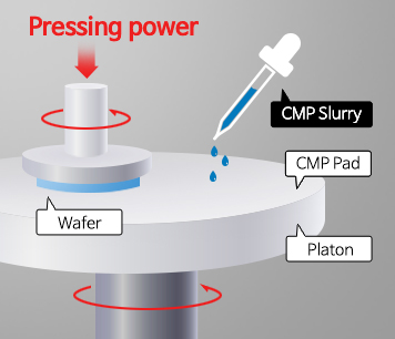
 CMP process
Usage
Wide planarization of semiconductor wafers
Adjustment of topology and surface roughness
Major products
| Major products | Features |
|---|---|
| SW-300 | Low defect slurry used in adjustment of semiconductor wiring process and surface roughness |
| NTS-300 | Possible to selectively polish the silicon nitride film (~1,000 A/min) and stop at the poly-silicon and silicon oxide films |
| SWC-100 | A colloidal ceria-based next-generation product with a low scratch, low dishing function |
| SAC-100 | The new work process uses amorphous carbon membrane, a next-generation material, to achieve a high polishing rate and low defect performance. |
| HTC-L-200 | Free adjustment of the polishing rate of Silicon Oxide, Copper, Silicon Nitride, products used in the TSV work process, according to customer requirements. |
Certification


contact
| contact | 담당자 | Tel | |
|---|---|---|---|
| Pad/Sluury | 김종우 PL | 031-240-0481 | jongwoo15@sk.com |
| Pad/Sluury | 권영필 매니저 | yp.kwon@sk.com | |
| Pad/Sluury | 권민균 매니저 | mingyun@sk.com |
contact
| manager | contact |
|---|---|
| Pad/Sluury 김종우 PL |
TEL 031-240-0481 jongwoo15@sk.com |
| Pad/Sluury 권영필 매니저 |
TEL yp.kwon@sk.com |
| Pad/Sluury 권민균 매니저 |
TEL mingyun@sk.com |
