Pad products used to enhance the level of integration of semiconductors
The CMP (Chemical Mechanical Polishing) Pad is designed to increase the integration of semiconductors by polishing the surface of semiconductor wafers physically and chemically. It is a consumable for which demand is growing due to the rapid increase in the production of 3D Nand Flash and such like.
Cases of application
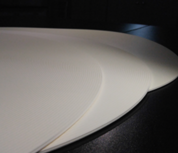 CMP Pad
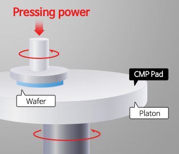 CMP process
Usage
Polishing the surface of semiconductor wafers
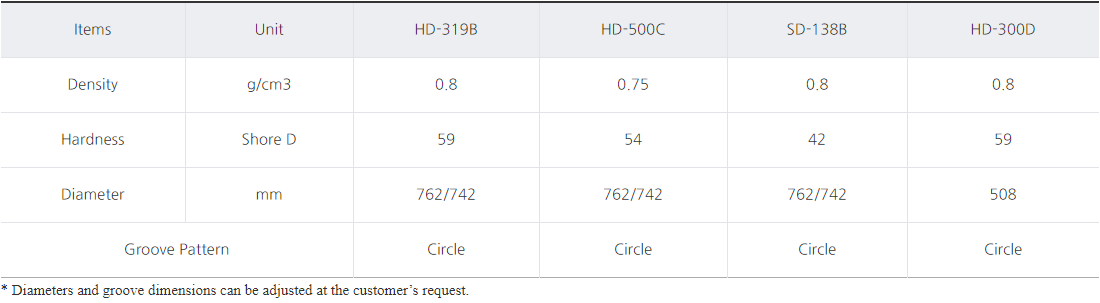
Major products
| Major products | Features |
|---|---|
| HD-319B | General purpose hard type of CMP Pad |
| HD-500C | Defect/scratch reducing hard type of CMP Pad |
| SD-138B | Defect/scratch reducing semi-hard type of CMP Pad |
| HD-300D | Hard-type CMP Pad for 200 mm wafers |
| Other | Dressing Pad for diamond disk quality inspection |
Packing unit
 Vacuum packing of each sheet → Delivery to customer businesses after packing
Table of physical properties of major products


contact
| contact | 담당자 | Tel | |
|---|---|---|---|
| Pad/Slurry | 김종우 PL | 031-240-0481 | jongwoo15@sk.com |
| Pad/Slurry | 권영필 매니저 | yp.kwon@sk.com | |
| Pad/Slurry | 권민균 매니저 | mingyun@sk.com |
contact
| manager | contact |
|---|---|
| Pad/Slurry 김종우 PL |
TEL 031-240-0481 jongwoo15@sk.com |
| Pad/Slurry 권영필 매니저 |
TEL yp.kwon@sk.com |
| Pad/Slurry 권민균 매니저 |
TEL mingyun@sk.com |
Download
Block B, The K Twin Towers, 50 Jongro-1-gil, Jongro-gu, Seoul, South Korea, SKC TEL: 02-3787-1234
Copyright by SKC. All rights reserved.